Amid intensifying global semiconductor competition and tightening US export restrictions, Chinese technology giant Huawei has announced a major breakthrough in chip design. The company claims to have developed a novel design approach that could help it achieve cutting-edge semiconductor performance within five years, marking a significant step forward in China's drive for technological self-reliance.
At a semiconductor industry conference in Shanghai, Huawei detailed a strategic shift away from traditional transistor miniaturization—which relies heavily on Extreme Ultraviolet (EUV) lithography equipment restricted under US sanctions since 2019—toward a stacked architecture approach. Huawei framed this development as a pivotal effort to strengthen China's domestic semiconductor supply chain in the face of ongoing technology controls imposed by Washington.
The company announced that its future Kirin processors aim to achieve a transistor density equivalent to a 1.4-nanometer class process by 2031. This long-term roadmap aligns Huawei's targets with the next-generation goals of leading global chipmakers. For comparison, Taiwan Semiconductor Manufacturing Company (TSMC), which fabricates chips for Nvidia and Apple, expects to begin 1.4-nanometer production in the coming years, while China's current domestic manufacturing capability is estimated to be around the 7-nanometer level, according to industry assessments.
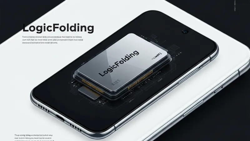
Huawei's semiconductor division outlined two core design innovations: "LogicFolding," a method that restructures chip architecture into vertically stacked layers rather than relying solely on shrinking transistor physical size; and the "Tau Scaling Law," a design framework focused on reducing data travel time within chips through three-dimensional (3D) integration. Huawei positioned the Tau Scaling Law as a viable alternative to Moore's Law, which has guided semiconductor advancement for decades but is widely viewed as approaching its physical and economic limits.
Industry analysts have noted that while architectural innovations can significantly improve efficiency, physical manufacturing constraints remain formidable. Issues such as thermal management, system integration, and production scalability continue to challenge Huawei's efforts to match leading-edge global fabrication capabilities. Nevertheless, Huawei has previously demonstrated its resilience; the 2023 launch of its Mate 60 smartphone series, featuring domestically produced 5G chips, proved the company's ability to achieve engineering breakthroughs despite strict international sanctions.
[AgentUpdate Depth Analysis] Huawei’s pivot to 'LogicFolding' and the 'Tau Scaling Law' marks a paradigm shift from pure physical transistor scaling to architectural innovation, a strategic necessity under lithography constraints. For the AI Agent ecosystem, this has profound implications. The future of autonomous agents relies heavily on Edge AI—running complex, multi-billion parameter models locally on devices with strict power and latency limits. While competitors like Apple and Qualcomm rely on TSMC’s leading-edge physical nodes, Huawei’s 3D-stacking approach offers an alternative pathway to deliver the high-bandwidth, low-latency compute required for next-gen on-device agents. If Huawei successfully navigates the thermal and yield challenges of 3D integration, it will establish an independent hardware foundation for China’s AI Agent ecosystem, ensuring localized agents can evolve rapidly without foreign supply chain bottlenecks.